[ instrument | DAQ || main help index ]
[ octopole | lens | emitter | channeltron | phosphor screen | geometries | practical hints | tweaks ]
The first SPA-LEED instruments were built by Leybold but discontinued in the 1990s. The latest version of the SPA-LEED instrument with a conical shaped front is available at Omicron NanoTechnology.

The simplest view of a SPA-LEED, which is nearly sufficient to work with, is the following: As in an optical LEED system, the electron gun sends an electron beam to the sample, the electrons are scattered and diffracted. In the SPA-LEED the diffraction image is scanned with a deflection system over a small detector and the count rate is recorded on a computer.
Note: The simple view is incorrect; in a SPA-LEED, no already existing diffraction image is scanned, but the combined deflection of incoming and diffracted electrons leads to the Ewald sphere construction of the SPA-LEED as described below.
Note: All references to Omicron manuals in the following
refer to Version 3.3 of the "Spectaleed Optics and Electron Gun Users's
Guide" [SOEG] and Version 1.7 of the "SPA-LEED Optics User's Guide" [SO].
The latest manuals are SpectaLEED V4.3, SPA-LEED V2.1 and all SPAiLEED
instruments are also supplied with with SPA-LEED user's guide V2.1, NGSPA SPA VOR and MUS V3.2,
NGLEED V3.2 and WinSPA Installation Notes V1.0 (as of October 8th 2009).
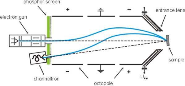
The SPA-LEEDs deflection system consists of three rows of electrostatic deflection units. This deflection system bends the electron beam in an S-shaped fashion, thereby changing its angle of incidence onto the sample while keeping the position constant at which the beam hits the sample.
Each of the three deflection units consists of eight deflection plates. Four of those form an x-y-deflection system just as an oscilloscope with cathode ray tube (CRT). Another four of the same geometry are aligned at 45 degrees to the previously mentioned four plates and each plate is kept on the intermediate electrostatic potential between its two neighbors (usually via resistive voltage dividers).
The front and the back deflection unit are oppositely connected to the deflection voltages and the middle deflection unit is kept grounded.
More detailed explanation of the functionality of the electrostatic deflection system of a third-generation SPA-LEED can be found in Percy Zahl's presentation at the 2008 SPA-LEED workshop.
While the electron gun lens could either produce a collimated (parallel) beam of electrons or focus the reflected electron beam on the channeltron's aperture, the additional electrostatic entrance lens around the front aperture of the SPA-LEED allows the production of very sharp diffraction images: The electron gun is used to produce a slightly divergent electron beam that is made parallel with the entrance lens (sometimes called "crystal lens" due to its proximity to the sample ("crystal")). The reflected electron beam comes off the sample also as a parallel beam that is focused onto the channeltron aperture during its second pass of the entrance lens. Therefore different electron gun and entrance lens settings have to be used in real-space and diffraction mode. In real space mode a convergent beam with a focus plane close to the sample plane and a switched-off entrance lens should be used.
Note: Simple adjustment hints can directly be derived from the operational principle:
In order to emphasize that the electron source in a LEED or RHEED system emits a directed and well-defined beam of electrons, those units are mostly referred to as electron guns. But don't call them like this in discussions with any customs officer when you have to transport your LEED system (to a beamline, for example); remember: it's an electron source!
Whichever type of electron emitter you have, a thorough outgassing before the start of experiments (especially after venting and bakeout of the UHV system) is mandatory; the small pumping cross section inside an electron gun increases the required pumping times. If the electron gun is not degassed properly it will send a beam of dirt directly onto the sample surface; sharp diffraction images of a clean Si(111) sample, for example, may vanish completely within a few minutes, even if the total system pressure is in the order of 10-10 mbar.
A tungsten filament is the most simple and inexpensive electron emitter. It is heated by direct current
to a temperature where thermally activated electrons can overcome the surface work function barrier
and pass into the vacuum (thermionic emission)
according to the Richardson-Dushman equation.
The main two drawbacks of thermal emitters are thermal and field
broadenings of the electrons' energy distribution as well as a reduced lifetime due to material evaporation and the
high reactivity of tungsten. In the daily use thermal emitters in scanning electron microscopes achieve
lifetimes of only a few hours at currents above 3 A, while the same emitters in a LEED system are operated at
below 2.5 A and usually survive a complete PhD thesis. The only mandatory precaution while using a tungsten filament
is a slow turnup: The filament tends to crystallize at high temperatures leading to internal stresses which can
cause a plastic deformation. Thus a simple switch-on should be avoided by any means. Instead, a current increase
of 0.1 A per each 10 seconds during the first turnup of a new tungsten filament
allows the relaxation of internal and thermal stresses without any deformation.
The more sophisticated version of tungsten emitter contains some Thorium for reduction of the surface work function. Typical operational data of a thoriated tungsten emitter (WTh) are
A lanthanum hexaboride emitter consists of a small LaB6 crystal which is for heating purposes mounted on a heating wire. The LaB6 crystal has a highly anisotropic work function and forms a sharp emission source if the crystal is correctly shaped and oriented. Typical operational data of a lanthanum hexaboride emitter (LaB6) are
The brilliance and emission current of those are unparalleled by any tungsten filament, even thoriated ones. Their main advantages are a sharper energy distribution of the electrons (less thermal broadening and no voltage drop over emitter) and a very high lifetime.
Note: An Omicron SPA-LEED is by default equipped with a high-quality LaB6 emitter.
For the LaB6 emitter in the Omicron third-generation SPA-LEED the following filament currents can be taken as a guideline (the values of your individual emitter are tabulated in a factory reference sheet delivered with your system): Filament standby current 0.600 A, operation current 0.900 - 1.150 A.
It should be noted that lanthanum hexaboride emitters require special precautions of the user. They are extremely hygroscopic (more than silica gel, which is usually used as desiccant)! Exposure to humid air should be avoided if possible: Vent your UHV system with clean and dry nitrogen gas and pump it to coarse vacuum whenever possible during maintenance periods. Furthermore, the surface of the LaB6 emitter can be poisoned irreversibly by some contaminants; for example, cleansing with acetone must be avoided for all parts inside the same vacuum chamber together with the SPA-LEED system. If the use of acetone is necessary in certain cases then all parts should get a thorough final rinse with propanol or ethanol before reassembly in the vacuum system. The next important aspect of LaB6 emitters is that they should not be exposed to air when they are hot; allow long cooldown times before venting the UHV system (more than 6 hours). After bakeout a slow turnup is recommended (0.001 A / s). If the emitter does not show emission after 1-2 days of degassing, a reforming of the crystal might be necessary. This is simply achieved by heating the emitter higher than for normal use. At elevated temperature and applied electrical field the crystal goes back to its equilibrium shape. Refer to the manual of your electron gun for further details.
The classic example of a single particle detector is the photomultiplier: An incoming particle (photon, electron, ion) hits an electrode at the entrance of the photomultiplier and removes one or several electrons from the bulk material into the vacuum. The electron(s) are then accelerated with a positive bias voltage to a second electrode. Since the electron(s) gained enough energy during the acceleration, each of them can then excite more than one electron from the next electrode. By using several subsequent accelerations and electrodes an avalanche of electrons is created from each incoming single particle. The bunch of electrons at the end of the photomultiplier is large enough to be detected as a current pulse.
A channeltron (channel electron multiplier) is a single particle detector based on the same principle of operation as a photomultiplier. Instead of the latter's discrete electrodes on increasingly positive electrostatic potential (dynodes) a channeltron consists of a continous tube that is internally coated with a low work function material (alkali metal) of high resistance (thin film). If a voltage is applied between the two ends of the channeltron, a continous voltage drop occurs over the whole length of the channeltron, corresponding to an accelerating field through the tube.
The curved and twisted design of a channeltron does not only increase the count efficiency by avoiding shortcuts for incoming particles but also largely reduces ion feedback. In a straight channel, positive charged ions would be able to gain energies of several hundred to a few thousand electron Volts and could cause serious damage by sputtering the inside of the detector.
In many applications a high angular and spatial acceptance
of the channeltron for incoming particles is desirable,
but not in the case of the SPA-LEED where an electron current
measurement at a well-defined point in (reciprocal) space is the objective (high spatial resolution = low spatial acceptance).
Therefore, in order to increase the spatial resolution of the channeltron
in the SPA-LEED an aperture is placed in front of its entrance.
As explained above, the instrument function of the SPA-LEED can not be sharper
than the virtual source diameter of the electron emitter.
Since the latter is about 100 μm for the LaB6
emitter employed, the aperture size of the Omicron SPA-LEED is also chosen to be
100 μm in order to match the virtual source diameter.
Note that a small aperture does not limit the angular acceptance
of the detector. This is necessary since in a SPA-LEED the incidence
angle of the scattered electrons changes with varying deflection voltages
as explained above.
A brief introduction to channeltron detectors can be found at Sjuts optoelectronics, a very detailed explanation of channeltron detectors is provided by Burle.
Channeltron single particle detectors are commercially available at several companies, for example Photonis (formerly Philips Photonics), Burle (formerly Galileo), k and m (ITT) and Sjuts, just to name a few.
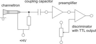
The amplifier for the electron avalanche has to be decoupled from the high voltage potential via a capacitor. A generic signal conditioning for a channeltron looks like this:
An example of the practical realisation of high voltage connection, decoupling and signal preamplification is this:
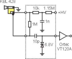
The circuit elements are a T-low-pass filter for the high voltage,
the RC-combination for HV decoupling and a suppressor diode for protection of the
fast amplifier (an Ortec VT120A in this case).
In your Omicron SPA-LEED system a different circuit is used. It is contained
in the "matching unit for SPA-LEED" (MUS).
The preamplifier should amplify the small voltage pulse caused by the electron bunch hitting the collector at the end of the channeltron to a suffient size to make further signal processing possible. The preamplifier must be placed as close to the channeltron as possible for achieving a high signal-to-noise ratio in the signal (a 30 to 50 cm long RG 58 cable from your SPA-LEED system is tolerable). In your Omicron system, the preamplifier unit is called VOR.
The signal conditioning consists of a discriminator and a TTL pulse former. The discriminator should suppress noise signals by comparing the incoming signal to a given threshold value. All pulses that pass the discriminator then have the same height, but their duration may be different. The TTL pulse former converts the very short pulses to pulses with a defined length that can be counted by the TTL counter in your data acquisition system.
A commercial signal conditioning chain may consist of a VT120 preamplifier, a 9307 discriminator and a 449 ratemeter for hardware online count rate monitoring, all available at Ortec.
With the availability of fast comparator integrated circuits cost-effective home-built solutions also become possible. In principle, the discriminator does only consist of such a fast comparator (such as the AD8561 , the Linear Technology LT1016 or the Maxim MXL1016), an adjustable stable voltage reference, a TTL pulse former and a 75 Ohm line driver.
Note: Pay attention to where the signal is a negative and where is should be a positive voltage pulse and choose inverting and non-inverting circuit elements accordingly. Using inverted pulses (such as negative NIM pulses ) with TTL 5V electronics may seemingly work, but will cause lots of troubles during debugging attempts.
A SPA-LEED has a flat phosphor screen for visual inspection of diffraction images. This is very helpful for basic alignment, quick focussing and debugging; in a well set-up system you'll probably need the phosphor screen only very seldom.
A SPA-LEED system can be used in two different geometries: The internal geometry with the sample almost perpendicular to the SPA-LEEDs axis and placed directly in front of the entrance lens, and the external geometry where an external electron gun is used as the electron source in a RHEED-like geometry and the SPA-LEED is "only" the detector. The external geometry was developed for the classic SPA-LEED system with a flat front in order to allow in-situ experiments during deposition or growth. The new Omicron third-generation SPA-LEED with its conical front makes the external geometry almost unnecessary, since sample access for evaporators is possible. "Almost", because some experiments require a smaller angle of incidence than possible in the internal geometry or a perpendicular (homogenous) deposition of material onto the surface.
A conventional LEED optics system (three or four grid LEED) is a real-space representation of the Ewald construction in reciprocal space:
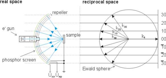
The ki-vector of the incoming electrons is always perpendicular to the sample surface. The elastically scattered (diffracted) electrons come off the sample with kf-vectors of the same length as ki, since the electron energy remains constant in elastic scattering. Diffraction intensity occurs when the diffraction condition is fulfilled, i.e., if kf-ki equals a reciprocal space vector of the lattice. The reciprocal space of a surface consists of lattice rods.
The principle of operation of a SPA-LEED is different. Both, incoming and diffracted electrons are deflected by the octopole deflector, keeping the angle between ki and kf constant. The radius of the Ewald sphere is nearly twice as large as in an optical LEED system at the same electron energy: Due to the small angle between ki and kf the radius is nearly 2ki. This makes the error from not straightening the diffraction images tolerably small.
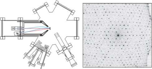
Note: SPA-LEED scans are not executed at contant kz!
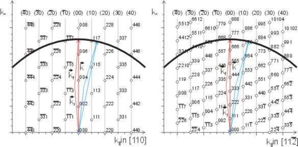
In the internal geometry, your sample is placed about 15 mm in front of and centered respective to the front lens of your SPA-LEED system. The working distance depends on the voltage ratio between front and rear octopole deflector and can - on cost of sub-optimum electron trajectories and thus reduced resolution - be changed with resistors networks instead of direct connection of the deflection voltages. The sample is slightly turned (or tilted, if you wish) in the direction of the connection line between electron gun and channeltron. With this angle you can centre the specular diffraction spot horizontally in your diffraction images. If you can also adjust the other angle of your sample holder system ("flip") then you can use that one for vertical centreing of your (00) diffraction spot.
A perfect mechanical alignment in internal geometry is when:
Note: If you have adjusted your system mechanically as described above you have optimum electron optical conditions. But: The (00) spot hits your channeltron if no deflection voltages are applied. This reduces its lifetime; even a longer lunch break may finish it off, if you have count rates in excess of 106 counts per second. You will definitely have to set the "beam parking position" in the software settings windows in that case!
In the external geometry the direction and energy of the incoming electrons from the external electron gun is constant. Only the diffracted electrons are deflected by the octopoles on their way to the channeltron.
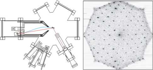
For the Ewald construction in the reciprocal space this has the following effect:
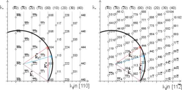
Diffraction images in the external geometry are more distorted than in internal geometry, the resolution is lower (broader spots).
A perfect mechanical alignment in the external geometry is similar to that described above for the internal geometry, with one difference: You may be able to tilt and turn the external electron gun relative to the electron detector which is obviously not possible with the internal electron gun of the SPA-LEED. This gives you the freedom to compensate for the gun inclination by changing the sample position and angles. Since you may end up with electron trajectories passing the entrance lens out of its centre, this recipe of adjusting the external electron gun is recommended:
Based on the previous explanations about physical background and the principles of operation of the components of a SPA-LEED, here are some hints to help with the daily lab work.
As is clear from the principle of operation of a channeltron, the user has to find the proper voltage to be applied to it. At very low voltages (say, below 1000 V) the channeltron is working on the edge of its f(U) curve. Low and unstable count rates are the result. The other extreme are very high voltages (above 3000 V) where ion feedback and additional avalanche effects (similar to field ionization) lead to a quickly diverging f(U) curve. The channeltron will be quickly destroyed in this region of operation.
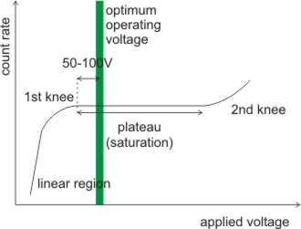
In between the two more or less well-defined "knees", a plateau of constant count rate independent of applied voltage exists. This is the region of safe and reliable operation. For minimum wear of the channeltron, select a voltage slightly above (50-100 V) the first knee.
Note: All voltages are examples only, the correct values depend on the type of your channeltron. Ideally, the manufacturer provided you with a "count rate versus voltage" curve of your channeltron in its "as manufactured" state. During aging the first kink voltage will increase, the second kink voltage decrease. As a result, the plateau region is reduced. The channeltron has to be replaced, if the plateau region is so small (maybe even non-existent) that no stable operational point can be found.
Hint: Write down the first edge voltage value frequently (weekly) into your lab book. Note the slow increase of that voltage. You will be able to determine if the end of the operational life of the channeltron is near.
Hint: Pay attention to the pressure of your UHV system during turnup of the high voltage at your channeltron after bakeouts. The channeltron may be hotter than the chamber due to weak thermal coupling and it may degas significantly during turnup.
The settings for repeller/suppressor, discriminator and Wehnelt are often mixed up,
since their effect is, on the first naive look, similar: There is no obvious effect on the
shape of a diffraction image and also the intensity is not affected over a certain range
of values, but suddenly the image intensity decreases dramatically.
But in fact, those three settings have nothing to do with each other and can
(and should) be adjusted independently:
The basic adjustment of your SPA-LEED system in diffraction mode is described above in the "entrance lens" section. Always remember how entrance lens and gun lens work together.
To optimize the settings of the gun lens(es) you have only to understand
the lens system and the lens voltage control of your Omicron SPA-LEED system
(the older Leybold systems have only a single electrostatic lens and therefore only one
"focus" knob to turn).
In the Omicron SPA-LEED electron gun three electrically charged rings with voltages L1, L2 and L3 form an
electrostatic lens.
The potential of L1 and L3 is the same. Consequently you have to deal with
two lens voltages, L1/L3 and L2.
Both of them are controlled with two knobs each, "offset" and "gain".
The idea is that the lens voltage is linearly increased with the electron energy,
described by a linear equation with offset and slope (gain).
Since the lens voltage at low energies (e.g., 50 eV) is largely
dominated by the offset and at high energies (200 eV) more by the gain,
you should iterate focusing with the two offset knobs at low energies and
with the two gain knobs at high energies.
Starting values without any guarantee for you particular system (length of SPA-LEED, sample distance) are: OffsetL2=4.06, GainL2=2.02, OffsetL1/3=2.39, GainL1/3=1.93.
If you are happy with the result, try to focus further by reducing the virtual source size of your electron emitter with the Wehnelt voltage. Don't spend too much time here, just increase the voltage just before the point where the electron beam current drastically decreases.
The preparation of clean and well-defined surfaces is highly non-trivial. Depending on the substrate material and even on the used surface analytical method different types of preparation may be suitable and promising. Many surfaces, especially metal surfaces, are prepared by alternating cleaning and annealing cycles: Removing contaminants from the surface (for example, by sputtering) and removing the induced defects are repeated. It is strongly recommended that you spend sufficient time for the development and/or optimization of a robust and effective cleaning recipe before starting deposition experiments. Also, checking the surface with a complementary method (for example with atomic force microscopy, AFM) will yield valuable, sometimes even shocking insights.
In the following, some advice will be given on the preparation of clean and well-defined silicon surfaces, because it is relatively easy, quick and inexpensive to produce highly ordered silicon surfaces (if your system allows high temperature heating of the sample).
You may cut your samples yourself from wafers by using a diamond glass cutter. In case you use pre-cut ("diced") wafers (which
is not very expensive and increases sample yield and reproducibility of the dimensions), they will likely be covered on one side with resist
and with a foil on the other. Remove a sample from the foil by slowly stretching the latter. Use titanium or Teflon tweezers, avoid stainless steel (see below).
Always use non-powdered latex or Nitrile gloves for your hands. Wipe off the resist thoroughly with an acetone-soaked
single-use cloth, such as a
KimWipe.
You may need several tissues. Do not scratch the surface by applying too much force.
The next step is to put the samples in an ultrasonic bath with propanol or
ethanol (pro analysis grade) for about 10-15 minutes.
If you insist on "perfectly clean" samples or if you cannot heat
the samples up to the melting point safely (e-beam heating), you
may want to use a wet-chemical cleaning method with hydrofluoric
acid (HF) or standard cleaning solutions from the semiconductor industry.
Details of wet chemical cleaning methods can be found in the publications
of Shiraki and Thompson (see reference section).
After that, mount the sample in your sample holder and put it in your vacuum system.
Degas the sample and sample holder for at least several hours at below 500°C
(the sample must be only just visible inside your UHV system, even in a fully dark room
with ion gauge and any other back light switched off).
The pressure must be better than 1x10⁻⁶ mbar.
Finally, remove the native oxide layer (if present, depending on wet chemical process)
along with surface contaminants by heating the sample to just below the melting point ("flashing"),
preferably by direct current heating, for 3..10 seconds at pressures below
1x10⁻⁸ mbar.
A rule-of-thumb is: A high temperature is more important than a low pressure.
The idea is to remove all surface dirt at once. Do not increase the current
too slowly: The surface contaminants (hydrocarbons) then do not
leave the surface quickly enough; they react with the Si and form stable silicon carbides (SiC).
If it is necessary (because the pressure rose to above 1x10⁻⁸ mbar), repeat this flashing procedure
1-2 minutes later one or two times.
If you have a load lock system and your sample size is
reproducible (due to dicing), it might be worth melting
one or two samples intentionally in order to test the maximum heating current.
The maximum flash current then is about 95% of the melting current.
It is recommended that you check the samples ex-situ with an AFM for
the presence of SiC clusters. A properly flashed Si(001) sample should appear
flat in the AFM, Si(111) surfaces show step heights of 3.14 Å.
Only 1-2 SiC clusters may appear on a 20x20 μm2 scan as small dots.
If you want to produce a very well ordered (7x7) reconstruction you should go through the phase transition at about 850°C
at a temperature ramp rate of about 1°C per second. To make this procedure not too time consuming, visually inspect the
diffraction pattern on the phosphor screen to determine the heating current near the phase transition and also the width
of this transition (20°C to 50°C). Thus the annealing of your sample at 850°C should not take more
than 1-2 minutes. There is no need for annealing procedures that take several ten minutes or even hours, since only the
width of the phase transition determines the duration. Take a look at real-time surface microscopy movies made by low
energy electron microscopy (LEEM) as an illustration of this fact, for example on the
homepage of the LEEM user community.
The (2x1) reconstruction of the Si(001) surface forms at much lower
temperatures and does therefore not need such an annealing.
Always avoid Ni and Cr contaminants on silicon surfaces (due to contact with stainless steel parts): They form stable surface reconstruction even at very small coverages!
Note: If you do not clean your sample properly and heat slowly up to the flashing temperature and choose a flashing temperature that is too low, you will produce a faceted surface with many SiC clusters. Such a surface can look spectacular in the reciprocal space map scanning mode, since it reveals all kinds facet rods (usually (115), (117), (119) for a Si(111) sample). Try it, if you are not familiar with RSM scans; the only thing you have to do is make every single possible mistake during sample preparation!
Again, also debugging may be a science of its own. In a SPA-LEED system, however, some typical "mistakes" always occur again and again; those should be given the first and foremost attention (the following list does neither claim to be complete nor to be ordered):
In the following, some suggestions for tweaking your SPA-LEED hardware to your
individual needs are described.
Those modifications were applied and successfully tested.
It should be noted, of course, that these
are just suggestions which have to be checked before applying them,
and that there will be no warranty or support of any kind be associated
with those modifications.
It is also important to understand that not all tweaks are useful for any user:
If also Auger electron spectroscopy (AES) should be performed with
the NG-LEED supply then a reduction of the primary electron energy range makes
no sense, if very high resolution LEED data is to be acquired with the
SPA-LEED system then the channeltron aperture should be left unchanged, etc.
Since SPA-LEED is not a very common surface science technique,
the control supply is not solely designed for the use
with a SPA-LEED. In case of very high demands on system performance
or ease of use the NG-LEED supply can be optimized for the use with a SPA-LEED instrument
via the following modifications. These modifications may be
carried out by the user on his/her own risk. All component names
and values refer to the nomenclature on the printed circuit board
"Control V3 (Omicron 07/98 AD)".
The energy range for LEED mode can be reduced to 0..500 V. This yields
a more precise setting of the electron energy. To accomplish this, a 10 kΩ
0.25 W metal film resistor should be soldered in parallel to the capacitor C40
(0.47 μF).
The suppressor voltage range can be increased to 80..120% of the energy voltage.
R125 (27 kΩ) to 20 kΩ, R126 (30 kΩ) to 20 kΩ.
It is highly recommended to use ten-turn potentiometers for all electron gun lens voltages, the Wehnelt voltage and the energy voltage.
Just replace the 270° potentiometers by ten-turn types of the same resistance.
For testing and optimising purposes it may be helpful to remove the RC combination for the channeltron voltage decoupling out of the UHV and place the components on the air side of the instrument. The additional 20 cm of unshielded cable length inside the chamber do not lead to a noticeable increase of electrical noise.
If faster measurements are desired on the cost of highest resolution, a widening
of the aperture in front of the channeltron can be helpful. Even 0.3..0.4 mm diameter
may not reduce the resolution of your system too much (depending on the crystalline
quality of the substrate): just calculate the physical diameter (FWHM) of the diffraction
spots, for example by measuring a spot-spot distance on the phosphor screen
and then by comparing with a line scan and using the rule of three. In most cases
you will see that a 100 μm diameter of the channeltron aperture (=instrument function)
will not even start to limit your overall resolution. On the other hand, a 300 μm aperture
diameter will give you 9 times the counts of the original one.
You will first have to remove the channeltron assembly (the system is assumed to be vented).
Then place a bright light source (halogen) lamp inside the chamber, make sure you can
see the small aperture clearly. Then use a sharp needle to widen the hole.
Do not apply forces! Instead, you can feel if you hit the original aperture.
Try to widen it by softly turning the needle. Frequently check the progress.
You may need 5-10 widening/checking iterations. Keep in mind: The human eye is quite sensitive!
If there is no visible increase of the brightness of the light through the
aperture, it will certainly not be too large.
Of course, you may as well look for commercially available exchange apertures with larger diameters,
but: That's too easy....
Some users have reported that channeltrons from Sjuts show significantly higher lifetimes in comparison to competitors, especially when using the channeltron at very high count rates (for example, with a larger aperture, see above).
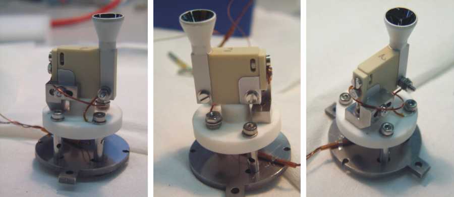
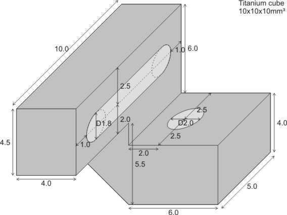
The type KBL428 can be monted in your Omicron SPA-LEED with a small adapter.
Front, back and collector voltage connections are self-explaining (see photos).
Note: New Omicron SPA-LEED systems are now supplied with a Sjuts channeltron. Replacement channeltrons are supplied fitted into the "channeltron box" - see the Omicron SPA-LEED Optics User's Guide Version 2.1.
The data acquisition hardware for the SPA-LEED is the Intelligent instrumentation PCI-20000 system (status: August 2009). It consists of a main carrier board and additional module boards for customized I/O capabilities. In the following some brief explanations will be given about installation and configuration of the PCI-20000 system for the use with a SPA-LEED.
WinSPA Software and Hardware Installation Notes Version 1.0 are supplied by Omicron NanoTechnology with all SPA-LEED instruments.
Note: In contrast to the hardware access of Spa4.1d with direct access to the PCI-20001 memory (with the good old MEM and MEMW structures), WinSPA needs an explicit readout of the counter activity for polling until the counter gate time has passed completely. The counter is active, as long as a second down-counter (defining the gate time) is running. This signal has to be fed back to one of the digital input lines. In order to do so:
WinSPA does not access the data acquisition hardware directly. Instead, the dynamic link library (DLL) SpaDAQ.dll creates an abstraction layer between WinSPA and the used data acquisition hardware. Therefore WinSPA can work with any suitable external hardware if a DLL with the required functionality is available.